Business
- XR (AR&VR) Micro OLED&Micro LED TFE Layer
• PECVD : SiNx, SiON, SiOx
• PEALD : SiOx, [SiNx], [Metal Doped Oxide]
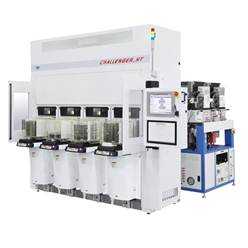
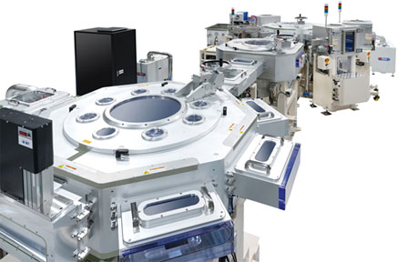
- Mass Production Equipment: 8 inch&12 inch
- SEMI Equipment Equivalent Performance & Size
- Particle Reduction Design
- Low Temperature OLED Encapsulation ≤ 85°C
- High Deposition Rate ≥ 300nm/min [PECVD]
- High Deposition Rate ≥ 7nm/min [PEALD]
- Self-Cleaning ALD Thin Film Encapsulation
- Excellent WVTR ≤ 1×10⁻⁵ g/m2·Day for Single Layer
- Excellent Uniformity ≤ 1% under
- oesales@hites.co.kr
XR (AR&VR) Micro OLED Backplane Layers
- PDL : Base of SiH4
- Black Layer : absorption factor ≥70%
- TEOS Gap-Fill and ETC.
- Mass Production Equipment: 8 inch&12 inch
- SEMI Equipment Equivalent Performance & Size
- Particle Reduction Design
- Process Temperature 70°C ~ 400°C
- Self-cleaning Availability with All Layers
- Verified Layer through Semiconductor Equipment
- ITO Film Damage Free
- Void&Seam Free
- oesales@hites.co.kr

- Metal Contact Cleaning
- ILD Undercut Free
- Native Oxide Removal
- Gas based Isotropic Oxide Etching
- In-situ or Separate Dry Clean
- High Speed Cyclic Etching
- Variable Selectivity to Nitride
- Oxide Patterning for 3-D Structures
- Metal Contact Cleaning
- ILD Undercut Free
- Native Oxide Removal
- oesales@hites.co.kr